Intel’s Ambitious Leap in Chip Packaging for AI
At the recent IEEE Electronic Components and Packaging Technology Conference (ECTC), Intel showcased groundbreaking advancements in chip packaging technology designed to meet the surging demands of artificial intelligence (AI) processing. As traditional means of chip development, like Moore’s Law, show signs of slowing, the tech giant is redefining how we think about silicon and its applications in AI.
Breaking the Silicon Barrier
The conventional size limit for a single silicon chip hovers around 800 square millimeters. As AI’s computational requirements escalate, manufacturers are looking for innovative packaging solutions that allow the integration of multiple silicon chips to function collectively. Intel’s recent unveilings focus on alleviating the constraints of traditional chip packages, significantly enhancing the possible silicon area within a single unit.
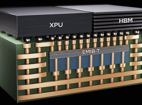
Among these innovations are improvements in how silicon dies—individual chips—are connected. The use of a small embedded silicon piece known as Embedded Multi-die Interconnect Bridge (EMIB) has evolved, now offering a new variant called EMIB-T. This version not only features fine horizontal interconnects but also introduces thicker vertical connections through a method called Through-Silicon Vias (TSVs). This enhancement lowers power loss and creates a more efficient path for energy delivery, which is crucial given the increasing power demands from AI processors.
Thermal Management: A Top Priority
As processors grow in size and capability, so too does the challenge of heat management. Intel’s solution lies in low-thermal-gradient thermal compression bonding, which allows greater flexibility in connecting silicon dies to organic substrates. By making the thermal expansion process more predictable, engineers can pack larger arrays of silicon dies together without compromising connectivity.
Additionally, the design and functionality of heat spreaders are set to improve. Intel’s approach involves assembling these components in parts rather than as a single unit. This strategy allows for better maintenance of flatness, ensuring efficient heat dissipation—a crucial factor for ensuring the reliability of high-performance systems.
Looking Ahead: Competition and Future Implications
While these innovations promise to transform AI chip packages and cater to the increasing computational demands of AI applications, they remain in the research and development phase. Intel did not provide project timelines or details on commercial availability, but the company recognizes the urgency of rolling out these technologies to remain competitive against rivals like TSMC, which is also expanding its packaging capabilities.
As AI continues to permeate various sectors—from healthcare to transportation—the need for advanced, effective processing solutions becomes ever more pressing. Intel’s focus on innovative packaging technology not only reflects the current trends in AI but also sets the stage for future advancements, potentially reshaping the landscape of computing in the coming years.
In this race to redefine chip capabilities, Intel’s latest developments highlight an exciting era of innovation that promises to bring us closer to achieving the full potential of artificial intelligence.

Writes about personal finance, side hustles, gadgets, and tech innovation.
Bio: Priya specializes in making complex financial and tech topics easy to digest, with experience in fintech and consumer reviews.

